


When an SPI sensor returns the wrong bytes, check the complete transaction against its datasheet before changing the calculation that uses those bytes. Verify chip select, clock mode, command and address bits, any required dummy phase, and the position of the returned payload. A readable logic-analyzer trace can still describe a transaction the sensor did not accept.
For a prototype review, ask for one annotated capture that connects the requested register to the bytes the application receives. That is more useful than a screenshot of a changing number. This guide concentrates on a low-voltage development board with an SPI sensor, not industrial wiring, a complete sensor-accuracy assessment or a universal driver implementation.
Write down the expected exchange first
SPI describes a clocked serial interface, but a familiar set of signal names does not establish a common register protocol. The selected device defines its command format, address width, transfer length and timing. Start with its current datasheet and the controller documentation, including any relevant errata.
Analog Devices’ introduction to SPI explains the relationship between clock polarity, clock phase and data sampling. Clock polarity determines the idle clock level; clock phase changes the sampling relationship. Record the actual sampling edge as well as the mode number so that the firmware setting, peripheral requirement and capture can be compared.
Prepare a short transaction specification:
- Which device is selected, its chip-select polarity, and its permitted supply and interface levels.
- Clock mode, bit order, word length and intended clock frequency.
- The exact command and address bits for one documented register read.
- Required clocks before useful data, expected payload length and byte ordering.
- Where chip select must remain active and the required timing between accesses.
Keep software buffer boundaries separate from wire boundaries. A driver may split a request into several transfers while the peripheral expects one uninterrupted chip-select interval. Conversely, a device may require a new chip-select event between operations. Check what the controller actually generates rather than inferring it from the number of API calls.
Find the payload rather than assuming byte zero
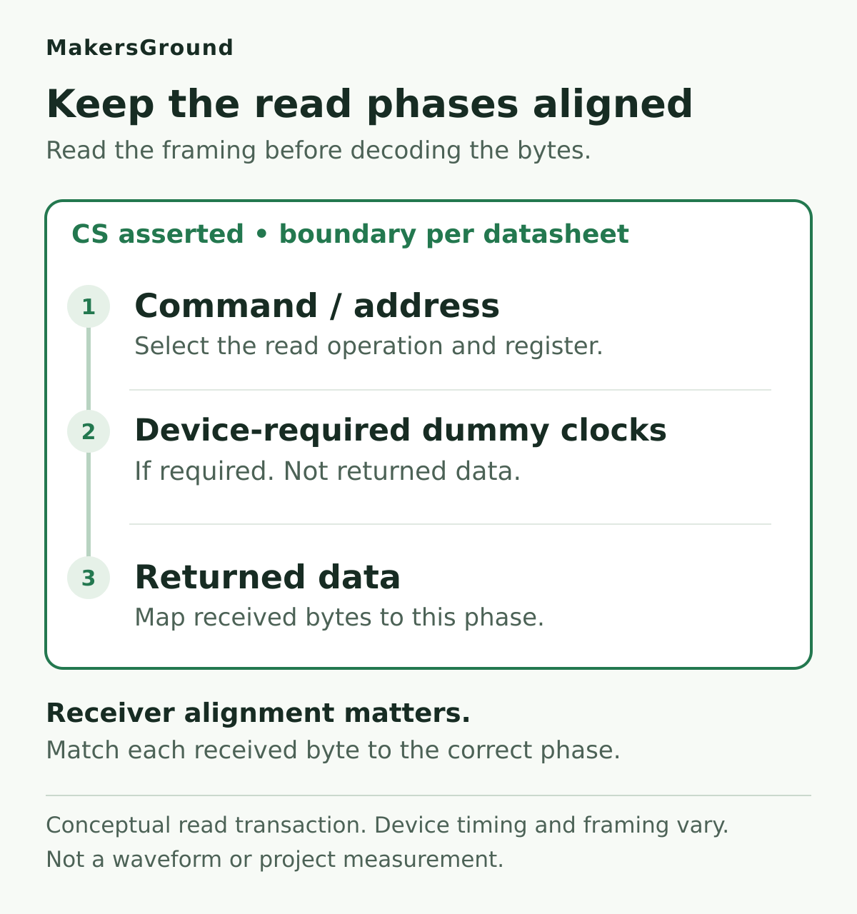
The controller receives bits while it generates clocks, including during command transmission. Those received bits are not automatically measurement data. The peripheral may need an address phase, dummy clocks or another documented delay before it drives a useful result.
The Bosch BMI270 datasheet, revision 1.6, gives a concrete example. Its normal SPI read includes a dummy byte after the command/address phase, before useful data. Its startup instructions also describe a preliminary read whose returned data is invalid while SPI is selected. These are different requirements: skipping the startup transaction does not eliminate the dummy byte from subsequent reads. The device supports modes 0 and 3, and its burst-read framing keeps chip select low. These details belong to the BMI270; they must not be copied to another sensor without checking its documentation.
Mark each phase on the capture and on the receive buffer. If firmware removes one byte too few or too many, a stable identity or plausible-looking sample can be assembled from the wrong positions. Check the mapping explicitly, especially when a driver combines command and receive operations or uses a wider controller word size than the sensor’s register width.
Capture the boundary signals together
Observe chip select, clock, controller-to-sensor data and sensor-to-controller data together. Select a trigger that includes the beginning of the access, and retain enough pre-trigger context to see the idle state. If the failure occurs only at startup, capture startup rather than a later transaction that already works.
Tektronix’s SPI decoding guide explains that channel assignments, thresholds, polarities and word size affect the decoder’s interpretation. Save those settings with the capture. A decode produced with the wrong mode can be misleading even when its hexadecimal display looks orderly.
Use the decoded values to navigate the evidence, then inspect the underlying signals. Compare clock periods, data setup and hold, and chip-select timing with the chosen device’s requirements. Evaluate the signal where the sensor receives it, not only beside the controller. A successful decode at the instrument’s threshold does not establish timing or voltage margin at the peripheral; this is an engineering inference from how decoding works, not a separate vendor guarantee.
Use appropriate probes, reference connections and a reviewed low-voltage setup. Probe loading and long temporary leads can change the signals being investigated. Our PCB test-access guide explains why the measurement connection belongs in the board review. Keep this test within the reviewed low-voltage setup; never defeat protective earth to make a measurement.
Build confidence one operation at a time
Start with a documented identification register after the required power-up and interface-selection sequence. Repeat the read and compare the complete expected value. A constant zero or all-ones result deserves investigation, but it does not identify a root cause by itself: selection, wiring, power, timing and buffer handling can produce similar symptoms.
Next, choose a documented configuration field that is safe to change in the development setup and supports meaningful readback. Check reserved bits and exclude write-only, self-clearing or read-side-effect registers from a naive equality test. Compare only the fields whose readback semantics are defined. This is a recommended test practice, not a claim that every device provides a suitable register.
Only then exercise measurement acquisition. Follow the sensor’s initialization, data-ready and sample-format requirements. Check signedness, byte order, scaling and freshness separately from bus transport. An identity read establishes evidence for that access; it does not demonstrate that the sensor is configured correctly or that a reported physical value is accurate.
A hypothetical shifted-read investigation
Consider a hypothetical monitoring board whose sensor identity is sometimes wrong and whose measurements occasionally look plausible. This is an illustrative investigation, not a MakersGround customer result.
The team first writes out the sensor’s required read phases. The capture shows that chip select covers the command and returned clocks, but the receive-buffer parser starts one byte before the documented payload. After correcting the offset, the team repeats the identity read, configuration readback and new-sample checks. It retains the original capture to show what changed.
That finding does not close the whole interface review. The corrected parser must also be tested at the intended clock rate and under normal system activity. A diagnostic run at a lower clock can help isolate a timing problem, but it cannot establish acceptance at the faster operating setting. Likewise, one successful read after a debugger pause does not verify the real startup sequence.
Keep a small acceptance record
| Check | Record |
|---|---|
| Transaction framing | Annotated command, dummy phase if required, payload and chip-select boundary. |
| Electrical timing | Observed signals, probe setup and comparison with device limits at the tested clock. |
| Configuration | Required initialization and meaningful field readback, with documented exclusions. |
| Application data | Payload mapping, units, signedness and evidence that the accepted sample is new. |
| Reproducibility | Board, sensor and firmware identifiers, document revisions, operating conditions and unresolved cases. |
Include repeated startup, normal concurrent activity and each supported bus configuration in the agreed test coverage. If several devices share the bus, verify selection and handover according to every device’s requirements. Do not extrapolate a single-sensor bench result to that arrangement without testing it.
Connect the board result to the product
MakersGround’s historical Gomicron engineering record documents our work across custom electronics, firmware and control, together with mechanical design, slicing software, prototyping and manufacturing. That cross-discipline scope is relevant when reviewing the boundary between a board and its embedded code. The record does not identify an SPI sensor, controller or bring-up method used in Gomicron.
For a custom electronics and PCB project, request the annotated transaction and acceptance record with the working prototype. Broader assembled-device measurement validation remains a separate task. Close this review when the selected device’s transaction, electrical requirements and application interpretation agree under the specified conditions, with remaining limitations visible.
Sources
Primary technical sources and linked company material checked on 29 October 2026. The test sequence and monitoring-board scenario are original engineering guidance and a hypothetical example, not measured project results. Manufacturer examples apply only to their stated devices and conditions.