


Before averaging readings from a multiplexed SAR ADC, verify that each retained conversion represents the selected input after the channel change. Test the actual acquisition interval, the source impedance and the scan sequence together. A quiet average can still contain a repeatable error inherited from the preceding channel.
Consider a hypothetical monitoring board with two stable analog inputs. Channel B reads differently when it follows a low voltage on channel A than when it follows a high voltage. That is a reason to investigate the acquisition path and channel-to-result association before tuning the display filter. It is not, by itself, proof of an ADC fault.
Separate acquisition time from conversion time
A successive approximation register, or SAR, ADC acquires an input onto a sampling capacitor before converting it. That capacitor must settle sufficiently close to the selected input during the available acquisition interval. Microchip’s acquisition-time explanation identifies source impedance, internal switching impedance and capacitance as relevant factors.
A slowly changing sensor does not remove this requirement. The sensor voltage may be steady while the ADC input repeatedly switches between different voltage levels. The electrical step seen by the acquisition circuit can therefore be much faster and larger than the physical quantity being measured.
Read the selected ADC or microcontroller’s timing diagram. Establish when channel selection takes effect, when tracking begins, when it ends and which conversion result belongs to which channel. A delay in the CPU program does not necessarily lengthen the ADC’s tracking window. Equally, an external multiplexer may be allowed to settle during another part of the conversion cycle only when that architecture and timing permit it.
Check the whole input path
The path may include a sensor output, protection components, a filter, a multiplexer and an amplifier before the ADC. Analog Devices’ multiplexed data-acquisition guide explains why the complete chain must settle, including the driver’s response to large channel-to-channel steps and charge kickback.
Do not replace that path with a convenient resistor-capacitor model without checking its assumptions. Amplifier slew rate, recovery, stability and output-current limits can matter. Adding a capacitor may help one disturbance while increasing settling time or creating a different loading problem. ADI’s multichannel optimization discussion describes those trade-offs.
For the hardware and firmware handover, record the ADC input circuit and the acquisition configuration together. Our hardware and firmware interface checklist covers the wider agreement about units, timing and data meaning. Here, the specific question is whether the selected channel has been acquired before its value is accepted.
Why five time constants can be insufficient
Hypothetical one-pole illustration: assume an ideal first-order response with an effective resistance of 10 kΩ and capacitance of 100 pF. Their product is a time constant of 1 µs. Assume the initial voltage step equals the full input span of an ideal 12-bit code scale, and allocate half an LSB to settling alone.
In this simplified model, the remaining error is the initial step multiplied by exp(−t/τ). At five time constants, the residual is about 27.60 LSB. Reaching half an LSB requires approximately ln(8192), or 9.01 time constants. At ten time constants, the residual is about 0.186 LSB.
ADI AN-1024 describes exponential settling and resolution-dependent time-constant requirements. Its table uses a one-LSB criterion; the half-LSB example here is separately calculated. Neither criterion is a universal acquisition setting.
This illustration excludes switch timing, amplifier slew and recovery, multiple poles, charge redistribution, reference behavior, leakage, ADC static errors, noise and component tolerances. It does not establish 12-bit system accuracy. Use the real component documentation and an appropriate error budget to decide what settling allowance the product can afford.
Keep the target input fixed and change its predecessor
Start with stable, independently checked input levels within the circuit’s permitted voltage and current limits. Define the allowed channel-dependent difference, required accepted-sample rate and latency before running the comparison. Use a suitable reference and account for its uncertainty. A longer acquisition setting is a useful diagnostic comparison, not an absolute calibration reference.
- Establish a single-channel baseline. Repeatedly acquire channel B without alternating to another input. Retain raw codes, settings and timestamps.
- Change the preceding channel. Hold B fixed, then alternate A and B. Compare B after a low A level and after a high A level. Include large legal voltage differences in both directions.
- Retain the sequence. Log the first and subsequent conversions after each switch, with their intended channel and actual acquisition settings. Check that firmware labels the returned result correctly.
- Sweep supported acquisition settings. Compare the raw results before changing the averaging filter. Record how the change affects the accepted per-channel rate and latency.
- Repeat with the intended hardware. Include relevant source impedances, input filtering, operating conditions and the production scan order. A low-impedance bench source alone may not represent the real sensor path.
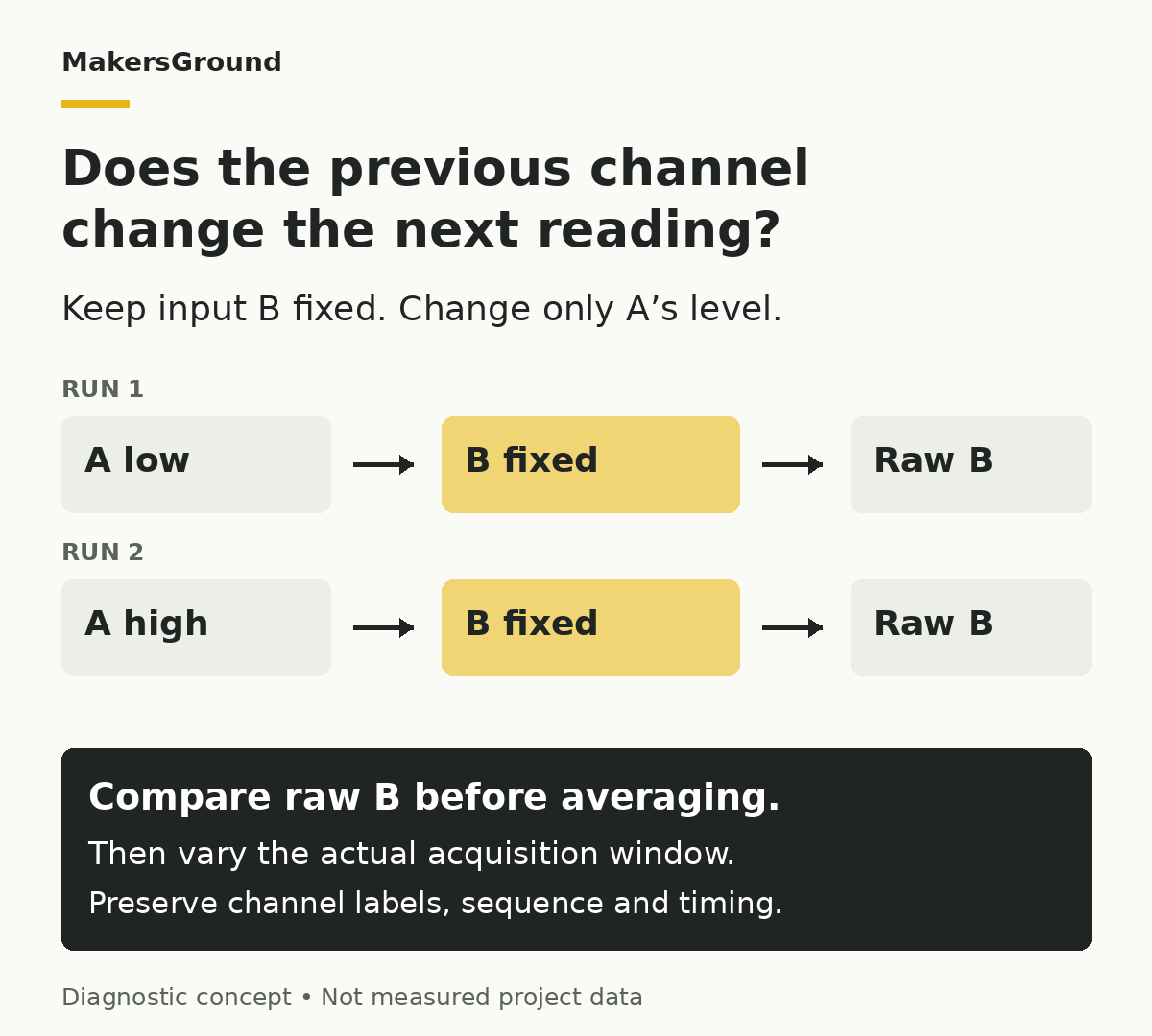
If B changes with A’s preceding level, inspect acquisition and the input chain, but also check scan indexing and result association. If a longer acquisition window reduces the difference, preserve that evidence and test the proposed final configuration. Do not silently turn the diagnostic setting into a released requirement.
Choose a remedy with a measurable trade-off
Possible changes include a longer actual acquisition interval, a lower scan rate, lower source impedance, a suitable buffer or revised input filtering. Each needs a hardware-specific review. A buffer adds power and its own errors; a different filter changes bandwidth and settling; a longer acquisition window changes throughput.
Discarding the first conversion is not a universal remedy. It is acceptable only when the selected device’s behavior and the retained samples have been verified, and the resulting throughput still meets the requirement. Count discarded samples when calculating the useful per-channel rate.
Averaging belongs after this investigation. ADI AN-2003 explains the assumptions behind reducing noise through oversampling and averaging. If every retained sample carries the same channel-dependent bias, taking their mean preserves that bias. That mathematical observation does not mean averaging can never change a transient; it means a calmer trace is not evidence that acquisition is correct.
Make the acceptance record reproducible
Keep the board and input-circuit revision, ADC identity, clock, acquisition settings, scan order, firmware revision, input levels, source impedances and raw data together. State which samples are retained, the useful rate per channel, the reference used and the conditions still untested. Preserve unsuccessful settings as diagnostic evidence rather than reporting only the cleanest trace.
Broader measurement acceptance still needs checks beyond the ADC. The assembled-device sensor validation guide addresses placement, reference comparisons, uncertainty and operating conditions. Passing this channel-switching test does not replace those checks.
Where electronics and firmware meet
MakersGround’s historical Gomicron engineering record documents our work across mechanical design, PCB electronics, firmware and control, slicing software, prototyping and manufacturing. It provides context for engineering decisions that cross board design and software boundaries.
That record does not identify an ADC architecture or publish channel-settling test results. The procedure and numerical example here are general engineering guidance, not a claim about Gomicron’s implementation or measured performance.
The useful release decision is specific: the retained sample sequence meets the agreed error, rate and latency requirements for the tested input path. Establish that result before relying on a smoother displayed number.
Sources
Technical sources and linked MakersGround material checked on 28 October 2026. The monitoring-board scenario and one-pole calculation are hypothetical.
- Microchip: ADC Acquisition Time.
- Analog Devices: Demystifying High-Performance Multiplexed Data-Acquisition Systems.
- Analog Devices: Performance Optimization of Multichannel DAQ Systems.
- Analog Devices AN-1024: How to Calculate the Settling Time and Sampling Rate of a Multiplexer.
- Analog Devices AN-2003: On-Chip Oversampling for the AD7380 Family of SAR ADCs.